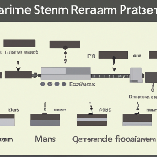
The Production Process of Mainstream Metal Film Resistors

I. Introduction
Metal film resistors are a crucial component in the world of electronics, serving as essential elements in circuits that control the flow of electrical current. These resistors are known for their precision, stability, and reliability, making them a popular choice in various applications, from consumer electronics to industrial machinery. Understanding the production process of metal film resistors is vital for appreciating their role in electronic devices and the technology behind them. This blog post will delve into the intricate steps involved in manufacturing mainstream metal film resistors, from raw materials to final testing and quality control.
II. Raw Materials
The production of metal film resistors begins with the selection of high-quality raw materials. The primary components include metal films, substrates, and protective coatings.
A. Types of Materials Used in Metal Film Resistors
1. **Metal Films**: The most common metal used in film resistors is a nickel-chromium alloy, known for its excellent resistive properties and stability. Other materials, such as tantalum nitride and carbon, may also be used depending on the specific requirements of the resistor.
2. **Substrates**: The substrate serves as the base for the metal film. Ceramic materials are typically used due to their thermal stability, electrical insulation properties, and ability to withstand high temperatures. The choice of substrate can significantly affect the performance and reliability of the resistor.
3. **Protective Coatings**: To enhance durability and protect against environmental factors, resistors are often coated with protective materials. These coatings can include epoxy or silicone, which provide moisture resistance and mechanical protection.
B. Quality Control of Raw Materials
Before production begins, rigorous quality control measures are implemented to ensure that all raw materials meet industry standards. This includes testing for resistivity, thermal stability, and mechanical strength. High-quality materials are essential for producing resistors that perform reliably over time.
III. Film Deposition
Once the raw materials are prepared, the next step is the deposition of the metal film onto the substrate. This process is critical, as the properties of the film directly influence the performance of the resistor.
A. Techniques for Depositing Metal Films
1. **Vacuum Deposition**: In this method, metal is vaporized in a vacuum chamber and then deposited onto the substrate. This technique allows for precise control over the thickness and uniformity of the film.
2. **Sputtering**: Sputtering involves bombarding a target material with high-energy particles, causing atoms to be ejected and deposited onto the substrate. This method is known for producing high-quality films with excellent adhesion.
B. Thickness Control and Uniformity
Achieving the correct thickness and uniformity of the metal film is crucial for ensuring consistent resistance values. Advanced monitoring systems are employed during the deposition process to measure film thickness in real-time, allowing for adjustments as needed.
C. Importance of Film Properties
The resistivity of the metal film is a key factor in determining the overall resistance of the resistor. The choice of metal and the deposition technique can significantly influence these properties, making careful selection and control essential.
IV. Resistor Patterning
After the metal film has been deposited, the next step is to create the resistor pattern. This process involves several techniques, primarily photolithography and etching.
A. Photolithography Process
1. **Application of Photoresist**: A light-sensitive material called photoresist is applied to the metal film. This layer will define the areas that will remain as the resistor.
2. **Exposure to UV Light**: The photoresist is then exposed to ultraviolet (UV) light through a mask that contains the desired resistor pattern. The areas exposed to light undergo a chemical change.
3. **Development of the Pattern**: After exposure, the photoresist is developed, washing away the unexposed areas and leaving behind a pattern that corresponds to the desired resistor shape.
B. Etching Process
1. **Wet Etching**: In this method, a chemical solution is used to remove the metal film in the areas not protected by the photoresist. This technique is effective but can be less precise than dry etching.
2. **Dry Etching**: This process uses plasma or reactive gases to etch away the metal film. Dry etching offers greater precision and control, making it the preferred method for high-density applications.
C. Finalizing the Resistor Pattern
Once the etching process is complete, the remaining photoresist is stripped away, leaving behind the final resistor pattern on the substrate. This step is crucial for ensuring that the resistor has the correct dimensions and shape.
V. Trimming and Calibration
After the resistor pattern has been finalized, the next step is trimming and calibration to achieve the desired resistance value.
A. Trimming Techniques
1. **Laser Trimming**: This method uses a focused laser beam to precisely remove small amounts of the metal film, allowing for fine adjustments to the resistance value. Laser trimming is highly accurate and can be automated for efficiency.
2. **Mechanical Trimming**: In some cases, mechanical methods may be used to trim the resistor. This involves physically removing material using a cutting tool, though it is less common than laser trimming due to lower precision.
B. Calibration of Resistance Values
Once trimming is complete, the resistors are calibrated to ensure they meet specified resistance values. This process involves measuring the resistance and making any necessary adjustments through trimming.
C. Importance of Precision in Trimming
Precision in trimming is critical, as even small deviations can lead to significant changes in resistance. High-quality resistors must maintain tight tolerances to ensure reliable performance in electronic circuits.
VI. Assembly and Packaging
After trimming and calibration, the resistors are ready for assembly and packaging.
A. Mounting the Resistors
1. **Surface Mount Technology (SMT)**: This method involves mounting resistors directly onto the surface of printed circuit boards (PCBs). SMT is widely used due to its efficiency and ability to accommodate high-density designs.
2. **Through-Hole Technology**: In this traditional method, resistors are inserted into holes on the PCB and soldered in place. While less common in modern designs, through-hole technology is still used in certain applications.
B. Protective Coatings and Encapsulation
To enhance durability and protect against environmental factors, resistors are often coated with protective materials. Encapsulation may also be applied to shield the resistors from moisture, dust, and mechanical stress.
C. Quality Assurance During Assembly
Quality assurance measures are implemented throughout the assembly process to ensure that all components are correctly mounted and functioning as intended. This includes visual inspections and automated testing.
VII. Testing and Quality Control
The final step in the production process is rigorous testing and quality control to ensure that the resistors meet industry standards.
A. Electrical Testing Methods
1. **Resistance Measurement**: Each resistor is tested to verify its resistance value. This is typically done using precision measurement equipment to ensure accuracy.
2. **Temperature Coefficient Testing**: Resistors are also tested for their temperature coefficient, which indicates how resistance changes with temperature. This property is crucial for applications where temperature fluctuations are expected.
B. Environmental Testing
1. **Humidity and Temperature Cycling**: Resistors undergo environmental testing to assess their performance under varying humidity and temperature conditions. This helps ensure long-term reliability.
2. **Long-Term Reliability Tests**: Additional tests may be conducted to evaluate the resistors' performance over extended periods, simulating real-world conditions.
C. Certification and Compliance with Standards
Finally, resistors must comply with industry standards and certifications, such as ISO and RoHS, to ensure they meet safety and environmental regulations. This step is essential for gaining customer trust and ensuring market acceptance.
VIII. Conclusion
The production process of mainstream metal film resistors is a complex and meticulous endeavor that involves multiple stages, from raw material selection to final testing. Each step is critical in ensuring that the resistors meet the high standards required for reliable performance in electronic circuits. As technology continues to advance, the demand for high-quality resistors will only increase, driving innovation in production techniques and materials. Understanding this production process not only highlights the importance of quality in metal film resistors but also sheds light on the future trends that may shape the industry. As we move forward, we can expect to see continued improvements in precision, efficiency, and sustainability in the production of these essential electronic components.
The Production Process of Mainstream Metal Film Resistors

I. Introduction
Metal film resistors are a crucial component in the world of electronics, serving as essential elements in circuits that control the flow of electrical current. These resistors are known for their precision, stability, and reliability, making them a popular choice in various applications, from consumer electronics to industrial machinery. Understanding the production process of metal film resistors is vital for appreciating their role in electronic devices and the technology behind them. This blog post will delve into the intricate steps involved in manufacturing mainstream metal film resistors, from raw materials to final testing and quality control.
II. Raw Materials
The production of metal film resistors begins with the selection of high-quality raw materials. The primary components include metal films, substrates, and protective coatings.
A. Types of Materials Used in Metal Film Resistors
1. **Metal Films**: The most common metal used in film resistors is a nickel-chromium alloy, known for its excellent resistive properties and stability. Other materials, such as tantalum nitride and carbon, may also be used depending on the specific requirements of the resistor.
2. **Substrates**: The substrate serves as the base for the metal film. Ceramic materials are typically used due to their thermal stability, electrical insulation properties, and ability to withstand high temperatures. The choice of substrate can significantly affect the performance and reliability of the resistor.
3. **Protective Coatings**: To enhance durability and protect against environmental factors, resistors are often coated with protective materials. These coatings can include epoxy or silicone, which provide moisture resistance and mechanical protection.
B. Quality Control of Raw Materials
Before production begins, rigorous quality control measures are implemented to ensure that all raw materials meet industry standards. This includes testing for resistivity, thermal stability, and mechanical strength. High-quality materials are essential for producing resistors that perform reliably over time.
III. Film Deposition
Once the raw materials are prepared, the next step is the deposition of the metal film onto the substrate. This process is critical, as the properties of the film directly influence the performance of the resistor.
A. Techniques for Depositing Metal Films
1. **Vacuum Deposition**: In this method, metal is vaporized in a vacuum chamber and then deposited onto the substrate. This technique allows for precise control over the thickness and uniformity of the film.
2. **Sputtering**: Sputtering involves bombarding a target material with high-energy particles, causing atoms to be ejected and deposited onto the substrate. This method is known for producing high-quality films with excellent adhesion.
B. Thickness Control and Uniformity
Achieving the correct thickness and uniformity of the metal film is crucial for ensuring consistent resistance values. Advanced monitoring systems are employed during the deposition process to measure film thickness in real-time, allowing for adjustments as needed.
C. Importance of Film Properties
The resistivity of the metal film is a key factor in determining the overall resistance of the resistor. The choice of metal and the deposition technique can significantly influence these properties, making careful selection and control essential.
IV. Resistor Patterning
After the metal film has been deposited, the next step is to create the resistor pattern. This process involves several techniques, primarily photolithography and etching.
A. Photolithography Process
1. **Application of Photoresist**: A light-sensitive material called photoresist is applied to the metal film. This layer will define the areas that will remain as the resistor.
2. **Exposure to UV Light**: The photoresist is then exposed to ultraviolet (UV) light through a mask that contains the desired resistor pattern. The areas exposed to light undergo a chemical change.
3. **Development of the Pattern**: After exposure, the photoresist is developed, washing away the unexposed areas and leaving behind a pattern that corresponds to the desired resistor shape.
B. Etching Process
1. **Wet Etching**: In this method, a chemical solution is used to remove the metal film in the areas not protected by the photoresist. This technique is effective but can be less precise than dry etching.
2. **Dry Etching**: This process uses plasma or reactive gases to etch away the metal film. Dry etching offers greater precision and control, making it the preferred method for high-density applications.
C. Finalizing the Resistor Pattern
Once the etching process is complete, the remaining photoresist is stripped away, leaving behind the final resistor pattern on the substrate. This step is crucial for ensuring that the resistor has the correct dimensions and shape.
V. Trimming and Calibration
After the resistor pattern has been finalized, the next step is trimming and calibration to achieve the desired resistance value.
A. Trimming Techniques
1. **Laser Trimming**: This method uses a focused laser beam to precisely remove small amounts of the metal film, allowing for fine adjustments to the resistance value. Laser trimming is highly accurate and can be automated for efficiency.
2. **Mechanical Trimming**: In some cases, mechanical methods may be used to trim the resistor. This involves physically removing material using a cutting tool, though it is less common than laser trimming due to lower precision.
B. Calibration of Resistance Values
Once trimming is complete, the resistors are calibrated to ensure they meet specified resistance values. This process involves measuring the resistance and making any necessary adjustments through trimming.
C. Importance of Precision in Trimming
Precision in trimming is critical, as even small deviations can lead to significant changes in resistance. High-quality resistors must maintain tight tolerances to ensure reliable performance in electronic circuits.
VI. Assembly and Packaging
After trimming and calibration, the resistors are ready for assembly and packaging.
A. Mounting the Resistors
1. **Surface Mount Technology (SMT)**: This method involves mounting resistors directly onto the surface of printed circuit boards (PCBs). SMT is widely used due to its efficiency and ability to accommodate high-density designs.
2. **Through-Hole Technology**: In this traditional method, resistors are inserted into holes on the PCB and soldered in place. While less common in modern designs, through-hole technology is still used in certain applications.
B. Protective Coatings and Encapsulation
To enhance durability and protect against environmental factors, resistors are often coated with protective materials. Encapsulation may also be applied to shield the resistors from moisture, dust, and mechanical stress.
C. Quality Assurance During Assembly
Quality assurance measures are implemented throughout the assembly process to ensure that all components are correctly mounted and functioning as intended. This includes visual inspections and automated testing.
VII. Testing and Quality Control
The final step in the production process is rigorous testing and quality control to ensure that the resistors meet industry standards.
A. Electrical Testing Methods
1. **Resistance Measurement**: Each resistor is tested to verify its resistance value. This is typically done using precision measurement equipment to ensure accuracy.
2. **Temperature Coefficient Testing**: Resistors are also tested for their temperature coefficient, which indicates how resistance changes with temperature. This property is crucial for applications where temperature fluctuations are expected.
B. Environmental Testing
1. **Humidity and Temperature Cycling**: Resistors undergo environmental testing to assess their performance under varying humidity and temperature conditions. This helps ensure long-term reliability.
2. **Long-Term Reliability Tests**: Additional tests may be conducted to evaluate the resistors' performance over extended periods, simulating real-world conditions.
C. Certification and Compliance with Standards
Finally, resistors must comply with industry standards and certifications, such as ISO and RoHS, to ensure they meet safety and environmental regulations. This step is essential for gaining customer trust and ensuring market acceptance.
VIII. Conclusion
The production process of mainstream metal film resistors is a complex and meticulous endeavor that involves multiple stages, from raw material selection to final testing. Each step is critical in ensuring that the resistors meet the high standards required for reliable performance in electronic circuits. As technology continues to advance, the demand for high-quality resistors will only increase, driving innovation in production techniques and materials. Understanding this production process not only highlights the importance of quality in metal film resistors but also sheds light on the future trends that may shape the industry. As we move forward, we can expect to see continued improvements in precision, efficiency, and sustainability in the production of these essential electronic components.


